Hasivo switches

Those DMAs (Bus Traffic Generators) actually look pretty powerful if they've still got the same capabilities that they had in the rtl8686 SoC

/* Generic DMA Control Register */
#define GDMA_MEMCPY			(0x0<<24)	/* Memory Copy */
#define GDMA_CHKOFF			(0x1<<24)	/* Checksum Offload */
#define GDMA_STCAM			(0x2<<24)	/* Sequential T-CAM */
#define GDMA_MEMSET			(0x3<<24)	/* Memory Set */
#define GDMA_B64ENC			(0x4<<24)	/* Base 64 Encode */
#define GDMA_B64DEC			(0x5<<24)	/* Base 64 Decode */
#define GDMA_QPENC			(0x6<<24)	/* Quoted Printable Encode */
#define GDMA_QPDEC			(0x7<<24)	/* Quoted Printable Decode */
#define GDMA_MIC			(0x8<<24)	/* Wireless MIC */
#define GDMA_MEMXOR			(0x9<<24)	/* Memory XOR */
#define GDMA_MEMCMP			(0xa<<24)	/* Memory Compare */
#define GDMA_BYTESWAP		(0xb<<24)	/* Byte Swap */
#define GDMA_PATTERN		(0xc<<24)	/* Pattern Match */
#define GDMA_SWAPTYPE0		(0<<22)		/* Original:{0,1,2,3} => {1,0,3,2} */
#define GDMA_SWAPTYPE1		(1<<22)		/* Original:{0,1,2,3} => {3,2,1,0} */
#define GDMA_ENTSIZMASK		(3<<20)		/* T-CAM Entry Size Mask */
#define GDMA_ENTSIZ32		(0<<20)		/* T-CAM Entry Size 32 bits */
#define GDMA_ENTSIZ64		(1<<20)		/* T-CAM Entry Size 64 bits */
#define GDMA_ENTSIZ128		(2<<20)		/* T-CAM Entry Size 128 bits */
#define GDMA_ENTSIZ256		(3<<20)		/* T-CAM Entry Size 256 bits */

There's a few other examples of more advanced possibilities for the GDMA engine, like for a regex and a few other Finite State Machine things, within the SDK.

I finally got around to putting a logic analyser on the board whilst it was running stock firmware.
Those little spring clips are pretty useful.

a. Revised after I discovered I had my GND reference hooked up to the +3v3 line.. only realised when trying to connect up console cable caused weird power dips.
a1.Showing the request/response format


a2. The request data (zoomed out)

a3. Request data (zoomed in), I couldn't get anything that didn't violate UART timing apart from 1 start, 9 data, no parity, 1 stop and at ~160000 baud. Maybe there is a combo that I'm not seeing that would work, but slower and less bits and the stop bit falls out of time, any parity bit mismatches on the 'inverted words'.

a4. Response data, which seems like standard 9600 1,8,N,1

Plugging in a PoE device to each port does present changing values in the response, one bit per port it seems. I was expecting some info on the total switch power, and per port current/power also however..

Incorrect stuff

a. The PoE signals look real weird. It's definitely a request/response type of communication. But it's not a standard UART signalling. It's a return to zero signalling of some kind. Each blip to the PoE controller is ~550ns wide, and each blip back is ~450ns wide (three images below of different zoom scales of the same waveform)

b. The LEDs are indeed serial shift register with the RCLK (register clock) triggered at the end

1 Like

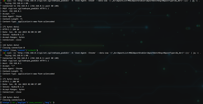
I finally received my S600WP-5GT-2SX_SE and I'm disturbed to learn there's pretty much no authentication to protect the configuration. Specifying a valid user-agent is sufficient authentication! :exploding_head:

Other issues:

  • Shipped the 1.25A@52V instead of the advertised 2.5A@52V power supply. :frowning:
  • Originally I had said some of my POE splitters didn't work, but they in fact do. I plugged them in wrong :upside_down_face:. All my POE devices work as expected.

Maybe this is a dumb question apologies as I cant find any answers anywhere.

I bought 2 2.5GB managed switches model S1100W-8GT-SE

I cant change the IP address or the default gateway. I figured out you can download the CFG file modify the IP address in the CFG file and then upload the CFG file and the IP address changes but the gateway will not. Once the device loses power the device goes back to 192.168.0.1

This is really frustrating as I dont use that IP address on my network. I want this device to use 192.168.3.5 and gateway of 192.168.3.1

Would be awesome if we can get some different useable firmware on these so I hope you folks are successful.

Wondering about this. Are you sure those adapters (and the USW-8-Lite POE) really are standard 802.3af or 802.3at?

The reason I ask is because of Ubuiquiti's history of passive PoE. And it's suspiciously hard to find the PoE specs for the USW-8-Lite PoE.The datasheet at https://dl.ui.com/ds/usw-lite-8-poe.pdf says "(4) PoE/PoE+ (Pins 1, 2+; 3, 6-)" without any spec reference. Could mean passive..

There isn't much help at https://help.ui.com/hc/en-us/articles/115000263008-UniFi-PoE-Availability-and-Modes either, stating bullshit like

Other vendors may refer to PoE, PoE+, and PoE++ as 802.3af, 802.3at, and 802.3bt respectively.

There's obviously more to the specs than max power. Stating 802.3af support has value in the sense that you can assume compatibility with other 802.3af equipment. Stating "PoE" support has no value whatsoever. The only reason to avoid referring to the standards is if they're not compliant.

This has confused and annoyed people for years. See for eaxmple https://community.ui.com/questions/US-8-60W-POE-specs-question/cafea97c-de88-4a49-b3a3-3b91659aed96

The U6-Lite makes this even more confusing. The datasheet is just as useless, claiming "PoE, passive PoE (48V)". But this device is actually a real 802.3af or at device. I have two of them powered by a ZyXEL GS1900-10HP.

So if would be good if you tested the Hasvivo with known standards compliant PDs. What kind of adapters are you using, and how do you know that they're not just taking passive PoE input? I'm sorry, but working with the USW-8-Lite PoE does not prove anything.

Another possibility is of course that the Hasvivo is delivering passive PoE. Which also should work with the U6 Lite according to the datasheet.

1 Like

Mine definitely lights up my 802.3af test adapter on all ports apart from Port 1, which is configured for 802.3bt. My adapter doesn't light up for this, but it's a reasonably cheap adapter.. so unsure if it's the adapter or the Hasivo 1100WP to blame in 802.3bt mode. I'd probably need another higher priced PoE 802.3bt switch before I could point the finger more definitively.

Yes, I screwed up. In a hurry I plugged both adapters in backwards. Was frazzled by the lack of HTTP auth and smaller PSU that I wasn't paying attention. I'll update my earlier post to strike through to not confuse others.

All POE devices I have (splitters, switches, APs) work.

I've now had all the LEDs working :slight_smile:
Only a couple of issues:

  1. I don't think the LED Sync setting should require a change to the driver (as I'm currently doing it), but should be possible entirely through DTS and pinctrl mapping. However the register for this is not the same as the regular pinctrl register. And if I add another then I get lots of other pinctrl entries... like this example when I set it up to have reg = <0x1800000 0x1000> in the pinctrl node of the DT.
    Is there a way to have all the various pinctrl registers mapped into the DT without using a custom pinctrl driver?
...
[   82.443786] pinctrl core: registered pin 10923 (PIN10923) on pinctrl-single
[   82.451474] pinctrl core: registered pin 10924 (PIN10924) on pinctrl-single
...
  1. It doesn't appear that my ledset0 settings are being picked up from the DT and applied in the driver. When I check after boot, the 24 shift register clock pulses are there, as is the register pulse afterwards, but the serial data is all '0's until I manually edit the set control registers to match the DT config.
  2. Once I've done this, it seems that the PHY link present indication is 'latching' instead of being applicable to the current link state of the port. i.e. I plug in a device to lan1 port, and it lights up. But when I remove the device the lan1 link light is still on. I have to do something like ifconfig lan1 down, ifconfig lan1 up to get it to update. I suspect this relates to the forced sds handling for the 2.5gbps RTL8221B PHY handling... but don't quite know where to tweak at this stage.
1 Like

If anyone has issues with DACs on the S600WP-5GT-2S+, I should note that the stock firmware has problems too!

There are tons of javascript errors in the stock firmware, one of which prevents altering IP address settings, so I had to do that via telnet (enabled through one of the menus). Also, note that the config doesn't actually save persistently when you apply it (likely to allow recovery if you goof); to save persistently, you have to specifically click the "save" menu item to copy the running-config to the startup-config.

With a 3-meter DAC, the port goes into a weird state where the far end sees the link up at 10 gigabits, yet no actual traffic goes through, and the port LEDs don't light up on the Hasivo. To make things work, I ultimately went with a 10Gbase-T module on one port and a 1-meter DAC on the other port.

Via telnet (since ssh is broken), here's show tech-support on my switch, with a few VLANs configured:
S600WP-5GT-2S+: show tech-support - Pastebin.com

1 Like

Saw this, did same workaround, thought it was just me. Also saw ssh was broken :roll_eyes:

I'm using a 1M H!Fiber DAC (‎CAB-10GSFP-P1M-30-Cisco-HF(EU)-C) with no issues.. yet.

Was also able to get a $15 refund for the 65W vs 130W misleading listing.

@DanaGoyette What PSU did you receive?

Looks like mine is 52V 1.25A. That's enough for my uses, but rather stupidly, the settings menu for PoE won't let you set the PoE limit that low. The minimum value it allows me to enter is 200W, even though the default was 65, which is treated as invalid.

S600WP# configure
S600WP(config)# poe-total_pwr
  <200-1200>  The PSE total power.
  <cr>

For anyone not familiar with this style of console, the way to get help is to start typing a command, and then press '?'. Instead of printing a literal question mark, it'll print some sort of help for the current command. You also have to save the settings you change, and if they're working (i.e. you haven't locked yourself out), do copy running-config startup-config.

you can do a single bit pinctrl; pretty much how the system-led is done

I am working on a pinctrl driver for our target, but its super messy, and relies on mfd/syscon a lot, as our registers are litterally plastered all over the place ...

When I tried that it went nuts with the number of 'pins'. The current pinmux has

reg = <0x1b00cc00 0x4>;

When I tried

reg = <0x1b000200 0xca00>;

It very much 'broke' with far too many pins definitions (I power cycled.. it got rediculous).

And from memory even

reg = <0x1b00cc00 0x4>,
      <0x1b000200 0x4>;

resulted in 64 pins being defined, as did having two pinmux sections (with their own reg ranges).

I'm probably just not knowledgable enough in how the pinctrl system is actually supposed to work (with pinctrl-single etc). Also unsure how a custom pinctrl would work that wouldn't require a separate 'driver' for each SoC package variant (which seems silly.. surely DT could specify them generically enough for 'all devices').

You are missing the key data in your examples of course :slight_smile:

I have done the same for the SDA pinmux in some work I'm doing locally; and it seems to work. Assuming you want to enable led-sync as non-gpio:

		pinmux_gpio_sel: pinmux@1b000200 {
			compatible = "pinctrl-single";
			reg = <0x1b000200 0x4>;

			pinctrl-single,bit-per-mux;
			pinctrl-single,register-width = <32>;
			pinctrl-single,function-mask = <0x1>;
			#pinctrl-cells = <2>;

			/* enable USB LED pin */
			pinmux_usb_led: pinmux-usb-led {
				pinctrl-single,bits = <0x0 0x400 0x400>;
			};

			/* enable LED sync pin */
			pinmux_led_sync: pinmux-led-sync {
				pinctrl-single,bits = <0x0 0x800 0x800>;
			};

			/* enable GPIO pins */
			pinmux_gpio_pin18: pinmux-gpio-pin18 {
				pinctrl-single,bits = <0x0 0x0 0x400>;
			};

			pinmux_gpio_pin19: pinmux-gpio-pin19 {
				pinctrl-single,bits = <0x0 0x0 0x800>;
			};
		};

Not sure if we can put multiple registers in a pinmux declaration (i think you can with the offset property though, but ignoring that, this should work?

Not sure what those slave-spi configuration pins are for. The most obvious is if this is the companion chip, but then there's nothing that would initialize it, as the master SoC needs to configure the slave over exactly these pins. Also, what's even more confusing, we have dedicate 0/1 pinmuxing of the slave pins. ALso you can only configure the CS it listens on, and the SDO it replies on, which can be any GPIO. So my guess is, the incoming clock+MOSI is fixed, selectable via strapping pins/eeprom; and by default will never reply (except on the fixed function pin) and will always listen (regardless of CS) until you send a message to set this pin up. In short; you don't have to care of register space overlap on this pin :slight_smile:

One thing that might require a dedicate realtek pinctrler is the 'strenght' etc settings, which are stored in different registers all together.

Also, I have to check if we can use syscon/regmap nodes with pinctrl-single. If so, everything can be done with the dts, but it would be super messy somehow for sure :slight_smile: 10 regmaps, 12 register entries etc. though that might be unavoidable regardless, as the register space is such a mess ...

Did you still have the pinmux for the GPIO0 LED (to take it away from SYSLED control) with that DT?
This is what I remember was my first attempt, and it ended up with two sets of 32 'pins'.. one for the SYSLED register, and one for the LEDSYNC register (each with 32 pins). Which just seemed like the wrong way to go about it..

I suspect the slave-spi mode may have been intended to use a tiny boot ROM. That would have just configured the slave-spi pins (unless it's possible to do this via at-boot pull-ups/downs). Possibly even by staggering reset release from a master controller it might have been possible to use a single tiny spi flash to configure a number of SoCs as slave SPI devices.

I haven't tried it :slight_smile: I don't know if you can invoke multiple pinctrl registers, but why shouldn't you? Where did you find the 32 gpio's on the sysled pinctrl? To eb fair, I wouldn't be supprised if it always maps something in the size of 'width', but only allows you to change whatever you have defined in the mask. In the end, it will have to map that single 'width' sized registers and access it with a read/write. You shouldn't however be able to access any of the other bits however, e.g. you can't export any other pins (well you can't anyways can you? well maybe for gpio's :p)

I'm sorry if I wasn't clear enough; as that is what I inteded to say :slight_smile: but check pis A1 - A5, those are fixed-function SLV SPI pins. So what's the purpose for the dynamic GPIO pins? Why configure them all if we have fixed-function devices.

Though one thing just occurred to me just now; totally off-topic; but if we can controll the switch over SPI, we can also control the other peripherials over SPI. e.g. SoC -register-> SPImaster -SPI bus-> SPIsave -register-> I2C master -i2cbus -> i2c peripherial :slight_smile:

Which none of our drivers are accounting for afaik; though I think it's easy with regmap, as you can do regmap-mmio, or regmap SPI in the same way ... but not relevant for the LED-sync discussion :smiley:

I'm thinking that a specific 930x-pinconf driver might be the best, which would capture all the spread out Pin Control aspects. Including both which alternative functions (JTAG/SPI/LED/I2C/MDX/MDIO) if any are mapped to which pins, and what the various slew / drive / schmitt settings should be.

I'm not sure how popular such a chip-specific pinconf driver would be in upstream however.
It does look like Nvidia Tegra stuff might be similar.. so I guess there are grounds for it.

I guess something similar would probably be desirable for the 931x also.

If I ever finish this DMA thing, then I might get started on such a pinconf driver (for the 930x).

I've got an opinion query regarding the DT layout for the DMA stuff... the 930x appears to have 3 DMA 'channels'.

Which would be a better DT layout for it?

Option A

		lx0_gdma: dma@144000 {
			compatible = "realtek,rtl930x-gdma";
			reg = <0x144000 0x23c>;
			clocks = <&ccu CLK_LXB>;
			interrupt-parent = <&intc>;
			interrupts = <12 0>;
		};

		lx1_gdma: dma@00a000 {
			compatible = "realtek,rtl930x-gdma";
			reg = <0x00a000 0x23c>;
			clocks = <&ccu CLK_LXB>;
			interrupt-parent = <&intc>;
			interrupts = <12 0>;
		};

		lx2_gdma: dma@018000 {
			compatible = "realtek,rtl930x-gdma";
			reg = <0x018000 0x23c>;
			clocks = <&ccu CLK_LXB>;
			interrupt-parent = <&intc>;
			interrupts = <12 0>;
		};

Option B

		lx_gdma: dma@a000 {
			compatible = "realtek,rtl930x-gdma";
			reg = 	<0x144000 0xa0>,
					<0x00a000 0xa0>,
					<0x018000 0xa0>;
			clocks = <&ccu CLK_LXB>;
			interrupt-parent = <&intc>;
			interrupts = <12 0>;
		};

I kind of like the first, because it makes it more obvious which DMA engines are which, and if the 931x / 838x / 839x families have separate IRQs per DMA engine it would allow for this easier (ditto if there are different bus clocks required for each DMA engine).

The biggest problem still is, that we'd almost need like some huge regmap that touches almost everything.

I have also started to look into SPI configurability, as there's a target that uses our chip as a SPI controlled chip; so that makes things less trivial.

without a doubt :slight_smile:

Having a big regmap (0x0204-0xcc00) that just has a few sparse "yes" registers seems doable.
I don't know of any limitations of having a big regmap range defined.
Or does it force exclusive access? (I've seen references to syscon in this context.. but in reading about that it's apparently equivalent to 'simple-bus' that we already have for the SoC bus... so maybe it's irrelevant, and we can already use the existing config around this).

I had thought this was part of the benefit of the regmap stuff. But I'm not sure how challenging the mapping through the SPI addresses to slave control registers would be.
It seems like caching, and more appropriate clock behaviour would be required, we can't just assume we have the clocks as we want it, since it would be set from whatever the vendor ROM was, and that would dictate what all the other timings are.

That Option A does make the use of virtual channels a bit more straight forward also. At this stage I think I'd only allow for 4 or so virtual channels per 'physical' channel. There's still a bit more working through on this that I've got to do...

It does exactly that :slight_smile:
and the way to work with this, is to define a 'syscon' node.

But then this doesn't protect you from invalid writes. E.g. if driver A needs exclusive eaccess to registers 1 and 2; and driver B just needs to change a bit in register 2; doing one giant regmap, means driver B (and C and D etc) all have access to reg 1, even they do not need it.

It's just really nasty. THe alternative is, have (for example the pinconf driver) 'link' (via phandles) to multiple other driver registers.

so the pinmux driver has a phandle to the I2C regmap, the SPI-slave regmap, the networking regmap etc etc.

We can isolate things somewhat of course. I've created a page to help create an overview. https://svanheule.net/switches/rtl93xx/gpio_space if you are curious.

Syson actually isn't what we are after (but we need to to create the regmap), but simple-mfd. Because in the end, we are creatnig a bunch of MFD's.

It is, but nothing supports this concept yet, and drivers to need to be able to setup for both access methods. for example, an SPI reg interface in the devicetree doesn't seem to be supporting a 'range' property (I haven't checked, but also don't have hardware to check). The verizon cable modem for example (check this forum) uses an rtl9301 in SPI mode. Since we thus already have a user for this, we need to develop with this in mind (but luckily it seems to be only for the 0x1b000000 based registers.

I don't think we can actually control the clock to the 'switch' peripherial, it runs at a fixed 2.4 ghz frequency afaik. But ultimately, 'we dont' care' as in, this is should be handled by the bring-up code (with strapping pins/small eeprom). The clock-controller in any case, doesn't seem to be sitting on the switch register space, but the PLL's afaik are, so those need to be configurable via this interface as well.

Yep, and then, the debuggin gstarts, causing mayhem :slight_smile: btw did you look at the LX4189 datasheet? It talks about the lexra bus controller (LBC) in detail.