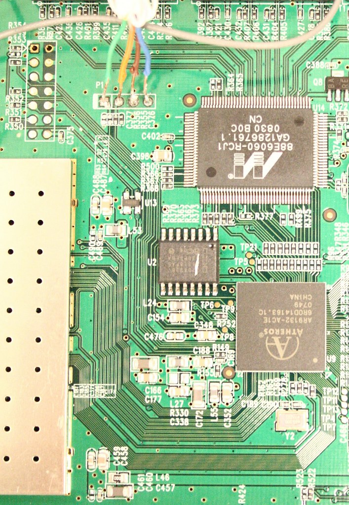
Does anyone know where the JTAG pins are located on a WNR2000 (FCC ID PY308200083)?
I want to patch the bootloader and be prepared in case I break it. There are no obvious pins rows.
I've found two test point groups on the back of the PCB:
- group 1: TP8, TP26-TP30 (six pins)
- group 2: TP2, TP12, TP16, TP18, TP19 (five pins)
so, assuming the JTAG pins are put closely together (not always true) and EJTAG requiring
five pins beside GND and Vcc (TDI, TDO, TMS, TCK and nTRST), while DINT and SRST are optional, both are candidates.
Unfortunately the traces on the PCB are difficult to follow towards the CPU.
Anyhow, it may be easier to replace the SPI flash by a socket.
The whole PCB, backside:
Group 1:
Group 2:
(Last edited by jal2 on 24 Mar 2010, 23:40)