Blueendless Kimax BS-U35WF - again

Hi,

I've got said Kimax HDD case / router. I know several topics involve this one, but all of them seem to revolve around a different version from mine. Originally, it sort of worked with its original firmware. My issue is that before installing OpenWrt, I upgraded the firmware to H1-1.7.5 from the link below. And since I did that, while the device boots and is accessible via the network, I can no longer log in, as it gives a "Router error(206)" to any password entered. I did do a factory reset several times (the 30-30-30 seconds rite), but that didn't help either. Additionally, I can't seem to find any contact points on the PCB which would possibly seem to be an RS232 port, so I can't attempt to revive it through the serial console. Any suggestions as to how I could flash this with OpenWrt from this state? I'm including all the details and board pictures below.

https://drive.google.com/file/d/1qsZrFEMhrZMB1fJUxEM4bnIYWr43tTyI

MCU: MT7620N
PCB1: 3.5wifi300M-20150723-2.0.
PCB2: HUI-300M-V1.1

1 Like

Absolutely no clue, anyone?

I was searching for the serial connection on this device. Found photos with a blue board and instructions, but it didn't resemble what is in my device. With an image search I found your post and those photos are exactly what is in my device...

Did you find the serial connection in the meanwhile? Looking at the board I don't see anything obvious. There are no test points as on the photos for the blue board. The processor is on the adapter board (4th photo in your series) and I'm now thinking to find the pins there and they see where they go. Hopefully through the 48 pins header...

Unfortunately, I haven't been able to make any progress with this ever since...

The board with the SATA connector is exactly the same and it seems that this one is similar across all variations. The board with the CPU, memory and flash drive looks at first glance the same, but in closer examination there are differences. Mine has three test pads, but all measure 0V. So that isn't very useful either...

I've found the datasheet for the MT7620 and it looks like we have the DR-QFN (12 mm x 12 mm) 148-Pin Package. I patched together the pin layout and rotated it so it's orientation is the same as in your 4th photo. The RX and TX are located at the top right corner near the two SMD resistors. Not sure if they are connected or if it is possible to expose them :thinking:.

When I got it -- only now I've some time to see if I can make something useful of it -- I have powered it up with the original firmware. So I can try to do the OpenWrt upgrade with there firmware and see if that works. But before I do that I want to see if I can dump the flash with an external flash programmer. It is the 8 pin chip on your 5th photo. It should als be possible to write a new firmware this way. I've not done that before, but I have one of these.

.

1 Like

Today I found my at least 25 year old microscope in the attic. With a 56x magnification I see the solder ball of pin 37 (RX) and it immediately connects to a via. On the other side the big 48 pins header covers the area, so no luck there. Pin 113 (TX) is staggered inside and almost covered by the chip I see another via. To me it seems that both RX and TX are connected? But where they go is still a mystery.
Next step is trying to make a good photo of my board so you can see it is slightly different than yours. Your photo is a bit out of focus in this area, but it looks identical to mine. Still lots of ideas, but other things have a higher priority for now. Just stay tuned...

Great work man, keep up! I won't be around to check this myself for another good month, but after that, I'll look into it!

I'm still thinking about which signals will be available on the 48 pins header. Most of the pins on the chip are for the SOC itself and for the DRAM. Both are probably not needed on a daughter board? I think DMA is not used? Else part of the pins for the latter are needed.

WiFi -- so most of RF part of the pins is also not needed, because the antennas are connected to the board with the SOC and DRAM. This SOC has an internal switch with five external ethernet ports. I think only one of those will be routed through the header.

Of course USB, LEDs and power are routed as well. But I think that leaves enough pins for serial and I2C. So there is still hope that we can finbd the serial on the header. To narrow it down I will make a better drawing of the pin layout and start poking from the daughter board. That will hopefully eliminate a lot of the 48 pins...

Mapping the pins is new for me, so please be careful when using the following information. Always check for yourself!

Starting with the SWAPnet NS681684 -- network filters for 10/100 -- I located the pins 17, 19, 21 and 23 on the header. I couldn't find the datasheet for the chip on our board, but I think the NS681680 should be the same. I created a new image from your second photo to show how I started numbering. Couldn't find any markings, but as long as we all use the same, there shouldn't be any confusion. Because the filters are essentially wires beeping says pin 1,2 and 3 are connected as are 6, 7 and 8. However the traces suggest that pin 17 on the header is RD-, pin 19 is RD+, pin 21 is TD- and pin 23 is TD+. I think we will find them going to the MDI_xx_P0 on the SOC.

I think pin 14 and 16 are going to the USB 2.0 end on the SOC, however because of the fine pitch this is difficult to measure for sure. SGM7227 is a fast switch to clean USB 2.0 signals if I understand the description correctly. GL850G is an USB 2.0 hub.

Pin 22 seems to be connected to the COM (= GND?) pins of the SATA connector. Because the SOC doesn't have any direct SATA pins, this probably goes through the chip at the bottom?

Pin 43 goes to R91 (220 ohm) and then to the top LED on the front panel. On its PCB this is labeled LED1 (power), but when I apply power LED2 lights up and its icon suggests that this is power. Which is confirmed in the manual. The other is WiFi and controlling that through the SOC is more logical.

Pin 46 goes to C65 and R1. The other end of the capacitor goes to the top left pin of the B1GDLK (6 pins) chip. Can't find any information about that one.

1 Like

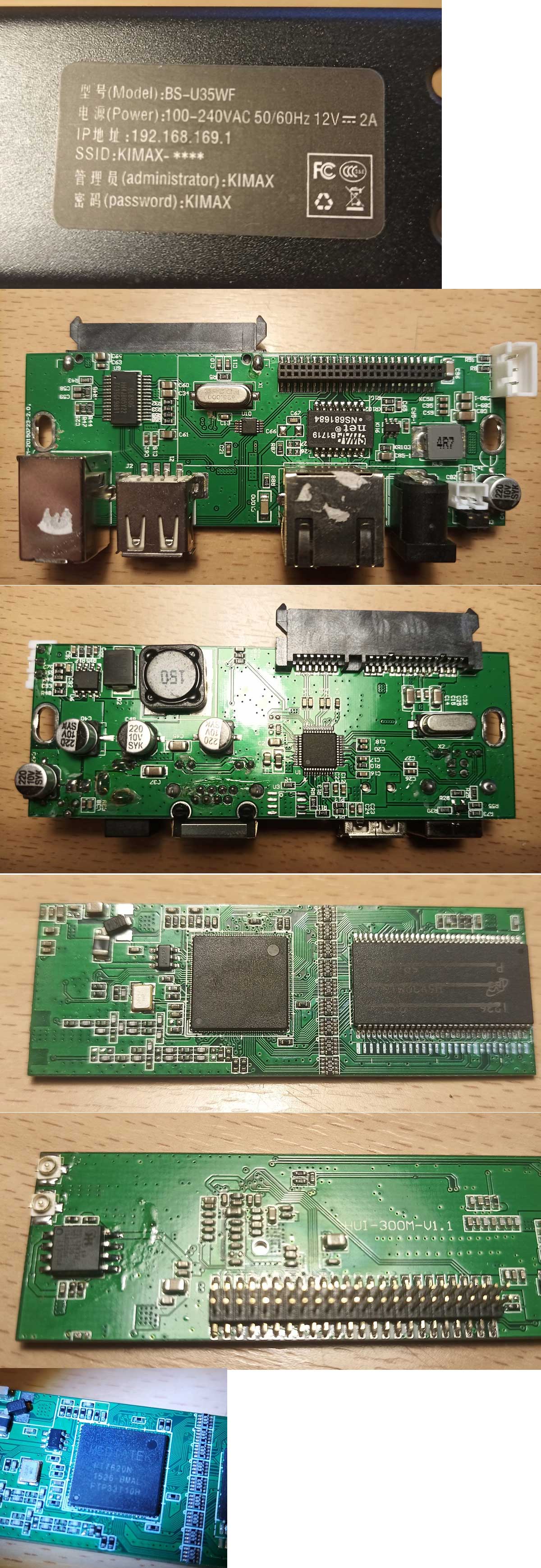
The chip at the bottom is an Initio INIC-3169PL and that is an SATA to USB 3.0 converter ASIC. Because the MT7620N only has USB 2.0 don't expect great performance :smile:. You can hardly call this a NAS combined with the 512 Mbit DDR SDRAM and 10/100 Mbit/s ethernet.

On the bottom of my SOC board is a KH25L12835F SPI flash chip which is 128 Mbit or 16 megabytes.

The only chip I can't identify is the 8 pins on the bottom of the board with the female header. I think it says AX5116 and I can find that on a Chinese website. But no datasheet.


Edit 2021-04-12T22:00:00Z

Good news and probably some bad news (for me at least).

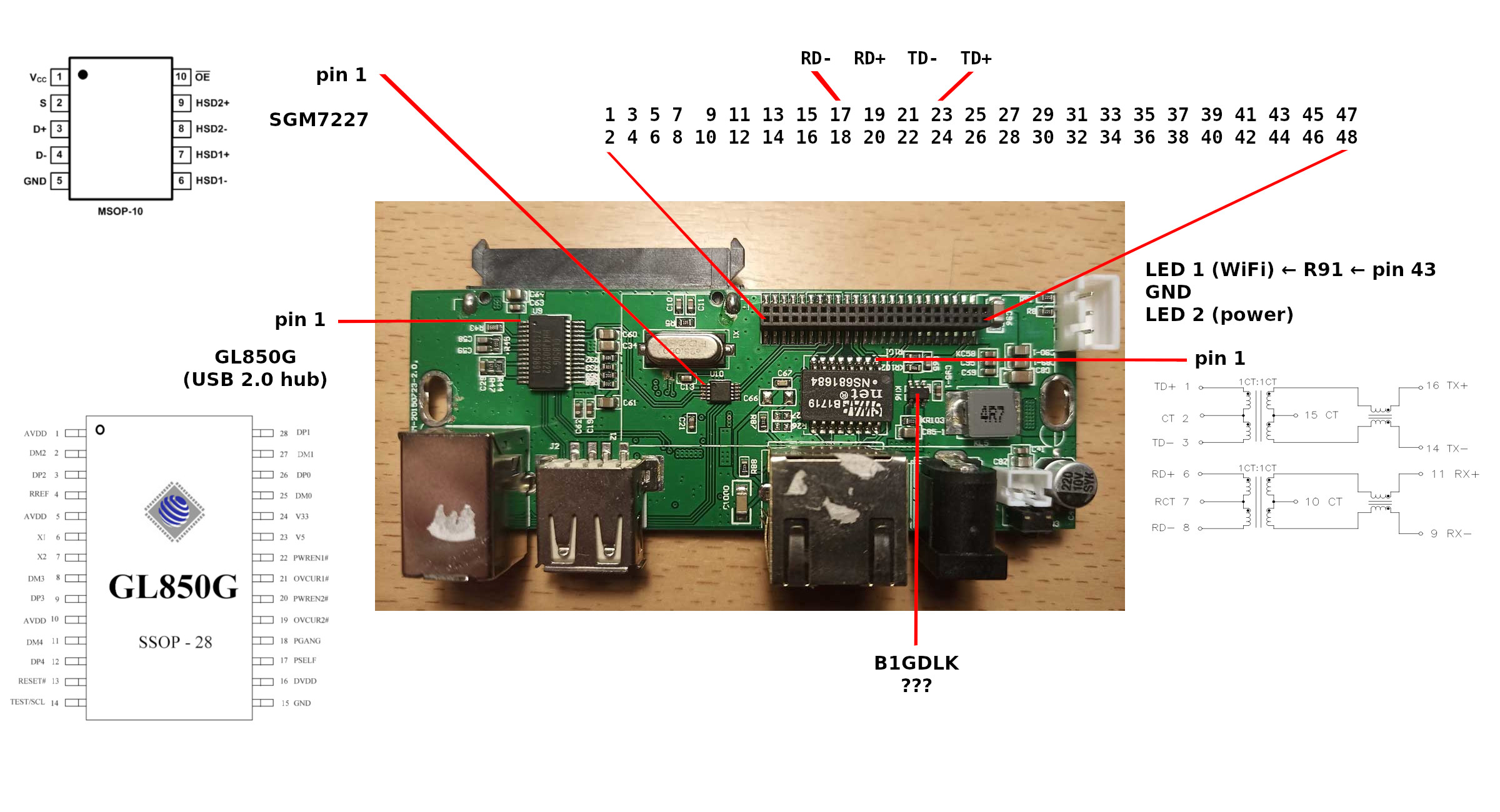
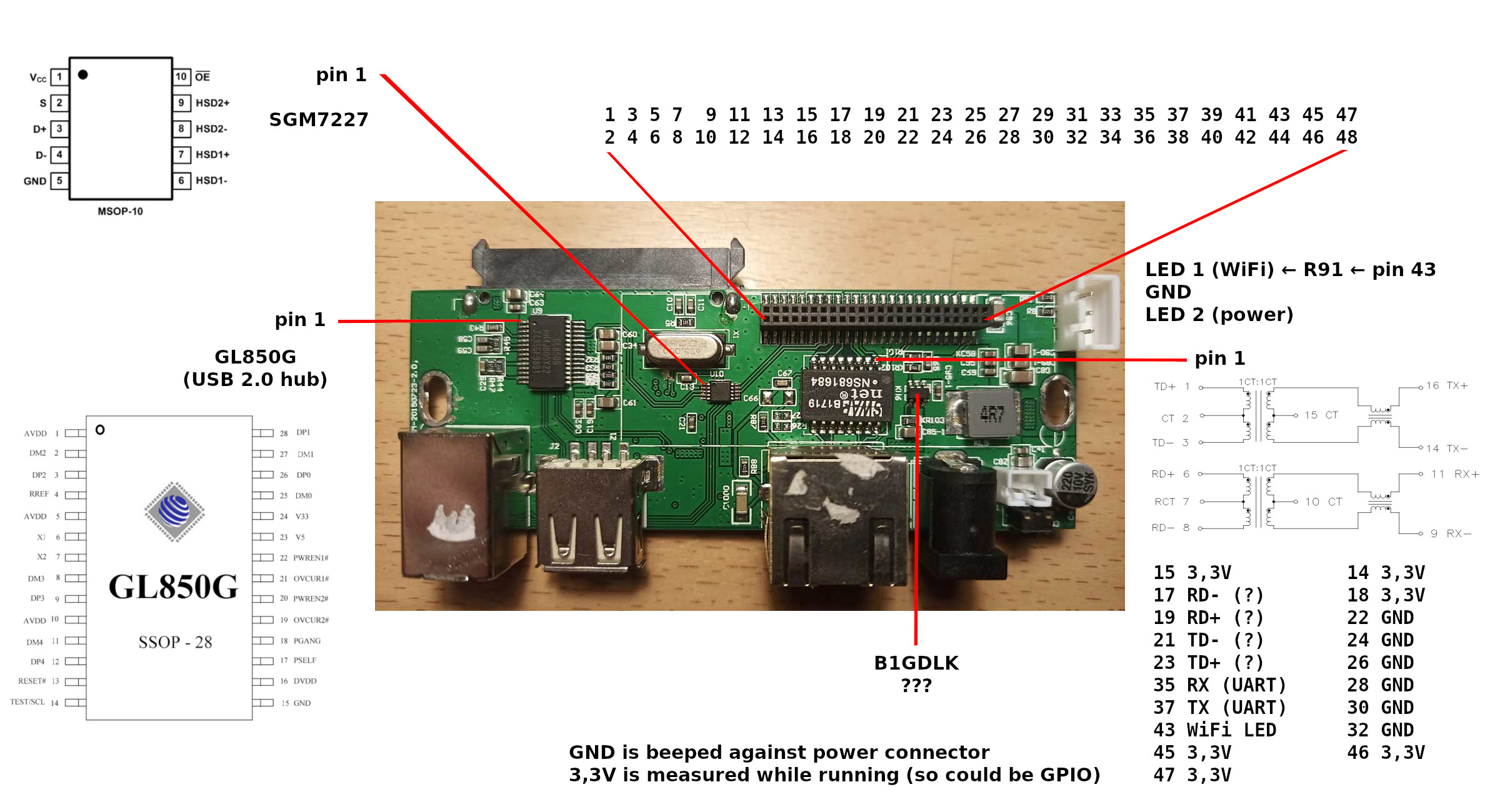
The good news is that I located the RX and TX pins on the header! I updated my information photo with all the details at this point. Again, only use this as a reference and always check yourself! I'm not responsible for any damage using my information. That said the TX on pin 37 gave this bootlog with 57600,8,N,1 as connection parameters. The RX pin is beeped to pin 35 but because of my current setup not confirmed by actual sending data to it. The bootlog has some useful information, but halfway through booting the kernel it stops. Not sure why, must investigate the last lines.

Then the bad news. I see some strange things which could have been caused with me poking around. This was the first time I did something like this, so it is a possibility although I was very careful. Anyway it still boots -- no harddisk connected -- and I see eventually the login screen. There the logo is a missing file and the information says it is damaged. Also I can't login, but no errors. I bootede it almost four years ago with an harddisk and I could login. I'm pretty sure I didn't change the password unless it was forced. I will try to reset it and check if a harddisk makes any changes. But the corrupted image and the warning in the bootlog that the rootfs has problems could mean a damaged flash?

As said, this machine is a joke for a NAS. Even when I bought it, I knew this was the case even when I didn't know that the advertised USB 3.0 is connected through USB 2.0 on the SOC. The main reason was an article how to replace the Chinese firmware for those who don't trust the installed version. So this machine has still use for a few other experiments. But that must wait because I will be receiving a few rescued boards from LG N2A2 NAS. Those are way more interesting :smile:.

I will try to put the information in the OpenWrt wiki. If I don't respond here, use the spam protected e-mail address on almost every page on my blog.

P.S. (time 15:52)
To proof that the RX pin is also found I soldered both connections to the header footings on the board with all the external connections. I also soldered a ground to the GND pin of the white three pin header which goes to the LEDs on the front. I typed 1 as choice and as you can see we can now upload images through TFTP to see if they work...

I recently got a BS-U35WF though it matches the one https://openwrt.org/toh/blueendless/u35wf so maybe not as much help here.

What I found is that the flashing instructions were not clear and actually incorrect. I made a backup of the flash chip first (SOIC 8 pin clip and RPi SPI reader) and tried the old way. I tried a few various methods, using the SPI to re-flash back to stock on failure, but the only one that actually worked was flashing the OpenWrt initramfs image from OEM webui, so that from there I could flash the sysupgrade image while NOT saving settings.

If you have a SPI chip reader to save the original full chip contents, you can try flashing this way.