And also I want to automate the installation of U-BOOT - at the result we just get an ELF image that needs to be loaded once via tftp and it writes U-BOOT where it necessary and blink the LEDs at the end of the process.
So you need to modify your U-Boot to the state of network support and the presence of a web interface.
And in about a week I can start back porting 88E6393X switch support from newer kernels to 5.10.
Let's not complicate it, for now, this is all just a start and I still cannot find how is the QCA8081 PHY managed nor what the SFP status GPIO-s are.
It's not directly on the MDIO bus of the SoC so I tried looking at the switch MDIO bus as it has a Clause 22/45 MDIO controller inside that allows you to connect an external PHY (Exactly what they are doing for the 2.5G QCA8081) but I cannot find it on any of the 0-31 addresses and I cannot figure it out from decompiled ROS drivers.
For the SFP I have a friend making me a PCB with LED-s that I can plug into the SFP port and then manually set GPIO-s to see which one is which signal as I only know the I2C GPIO pins (And that is working)
U-boot will most likely require some kind of a default config for the switch to just forward traffic as it intermittently works even now.
But I would like to get Linux/OpenWrt fully working first and only then complete the U-boot with the finishing touches.
But the web interface for U-boot is a no-go, there isn't any kind of generic support for the HTTP stack nor there is an HTTP stack that is small and up to date to be integrated into U-boot, for start just enabling netconsole so the U-boot is available via the network is fine enough.
@adron What is the -i arg in your kernel2minor doing?
I see that it's creating something similar to the stock boot partition
To me it seems like they have changed the YAFFS format used, now the kernel is just a file inside of the FS
-i - add image info block. it was needed for the first version of flashing script and then it was not used. Yes, you rightly noticed that the stock firmware most likely also has a similar info block. But I don't know what format it has. I think this was done on purpose so that nothing extraneous was launched on their devices.
Actually, the YAFFS itself starts from: 01 00 00 00 . 01 00 00 00
Yeah, it's just so weird.
BTW, the YAFSS patches are in the GPL.
To me, it's weird that there is no YAFFS magic 0x5941ff53 anywhere in the boot dump.
Nope, I am dumb due to endianness its reverse, and it exists at 0x14.
Could the bytes before be some kind of flag?
Take a look at yaffs_packedtags2.c
+/* This code packs a set of extended tags into a binary structure for
+ * NAND storage
+ */
+
+/* Some of the information is "extra" struff which can be packed in to
+ * speed scanning
+ * This is defined by having the EXTRA_HEADER_INFO_FLAG set.
+ */
+
+/* Extra flags applied to chunk_id */
+
+#define EXTRA_HEADER_INFO_FLAG	0x80000000
+#define EXTRA_SHRINK_FLAG	0x40000000
+#define EXTRA_SHADOWS_FLAG	0x20000000
+#define EXTRA_SPARE_FLAGS	0x10000000
+
+#define ALL_EXTRA_FLAGS		0xf0000000
+
+/* Also, the top 4 bits of the object Id are set to the object type. */
+#define EXTRA_OBJECT_TYPE_SHIFT (28)
+#define EXTRA_OBJECT_TYPE_MASK  ((0x0f) << EXTRA_OBJECT_TYPE_SHIFT)
I think everything is much simpler there. Yaffs is just the most common. 2048 bytes for data block and 64 bytes for oob. To create a kernel image via kernel2minor for this Yaffs, you need to run the following command: kernel2minor -k $KERNEL -r ./nand-yaffs2.bin -s 2048 -c and then write it to /dev/mtd0(without offset!). And it should work - but I haven't tested it 
At first I thought that there was some kind of secret info block, in fact, only the kernel and the VERSION file were written there. It's just that the kernel blocks start not from the beginning, but from the middle of the section (from about 35%) and the rest of the kernel goes from the beginning.
Yes, there is little endian - the order is the opposite of what was on the mips systems! Therefore, kernel2minor should be called WITHOUT the -e parameter.
Yeah, that was the first thing I tried.
Just running kernel2minor with -s 2048 -c and then using flash_erase /dev/mtd0 0 0 to wipe the partition and then nandwrite -o /dev/mtd0 on it.
But after rebooting it failed and pulled the u-boot ELF from bootp.
Is the packed image supposed to have the YAFFS magic cause it looks like it starts with the filename and I cannot find the magic and ROS is not happy at all with it:
[   19.917877] yaffs: dev is 32505857 name is "mtdblock1" rw
[   19.917881] yaffs: passed flags ""
[   19.917885] yaffs: yaffs: Attempting MTD mount of 31.1,"mtdblock1"
[   19.917889] yaffs: auto selecting yaffs2
[   19.961958] yaffs: yaffs_read_super: is_checkpointed 1
[   19.963322] yaffs: dev is 32505856 name is "mtdblock0" rw
[   19.963325] yaffs: passed flags ""
[   19.963329] yaffs: yaffs: Attempting MTD mount of 31.0,"mtdblock0"
[   19.963332] yaffs: auto selecting yaffs2
[   20.042934] yaffs: 36 blocks to be sorted...
[   21.017948] yaffs: yaffs tragedy: Bad type, -1862204424 != 15, for object 960 at chunk 128 during scan
[   21.075815] yaffs: **>> yaffs chunk 64 was not erased
[   21.076329] yaffs: **>> yaffs write required 2 attempts
[   21.081519] yaffs: yaffs_read_super: is_checkpointed 0
I was crazy enough to try and compile mkyaffs2image tool, off course they hacked way to hard so it doesn't compile at all
It is clear, then they all the same changed something in the 7th version of RouterOS for Yaffs. As soon as I am have a free time, I will try to understand what exactly and fix it.
Thanks, I will see how can I figure out where the hell is the QCA8081 connected.
Ok, so I went about trying the yaffs2utils which compile, but the generated image is pretty much what kernel2minor generates and nothing like the dump, for one the magic is still missing.
2 Likes
I googled a little here and draw. Hope this helps in your research.
QCA8081 electronic circuit example.
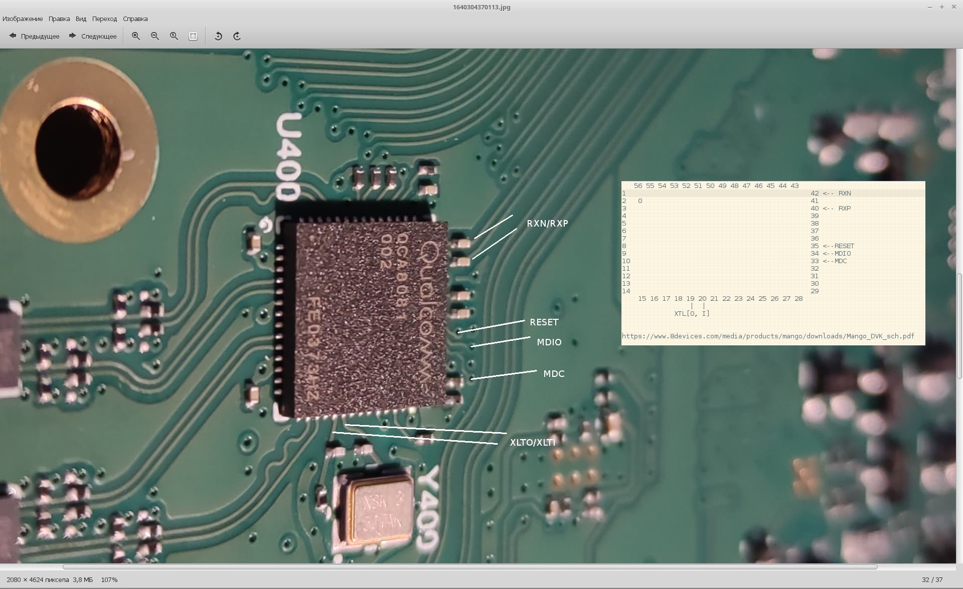
Thanks for mapping the pins, I even have the QCA8081 datasheet but for me, it's annoying as it's on the bottom of the PCB.
Damn, MDIO pins and the RESET go to a VIA, good luck tracing that, this would indicate that they are not connected to the switch but rather the SoC MDIO.
Would it be possible for you to measure if the QCA8081 MDIO pins are connected to the SoC MDIO on the switch pins?
I have the datasheet and can provide the pinout.
Nah, you cant actually do that as the switch is a BGA and the MDC/MDIO pins are in the third row of balls.
One could also manage the QCA8081 via I2C but I don't see anything on the single I2C bus
Yes, I also think that they are connected to the SoC GPIO. It remains to find out exactly which pins!
Well, you can grab the pins of the QCA8081 microcircuit with a tester's tip and bitbang the SoC GPIOs to see if a HIGH level is appears on them or not.
Then it's not on the HW MDIO bus as I only see the switch there, so it could be a bit-banged MDIO.
My issue is that I don't have fine enough multimeter tips and my logic analyzer probes don't fit as well.
I guess scrapping the vias and soldering a jumper wire for probing will be the only way to go. I'm trying to procure a unit as well and could help doing that.
2 Likes
It would probably be easier to solder some transformer wire to the pin pad than the via, it looks to be larger.
I don't have the equipment to do this, this is really microscope territory.
EuroDK had RB5009 in stock lately.
Luckily, mid last year I upgraded my home office with a nice professional soldering station, binocular and a pro logic analyser (the deep buffer, 16 channel, 1 GHz model). So this should really not be a big deal. Let me order my device later today...
2 Likes
Awesome, thanks.
I don't really solder anything much except for UART headers so I just use a Pinecil and 858D hot air station.
Got the Saleae Logic 16 Pro recently at work, now just gotta find something to reverse engineer
Yeah, sounds really challenging ![]() .
.
BTW: Do you have any experience in sniffing SGMII traffic? I was wondering if one could just hook up say another GMAC to some proprietary Cisco hardware and listen to what exactly they do on the wire.